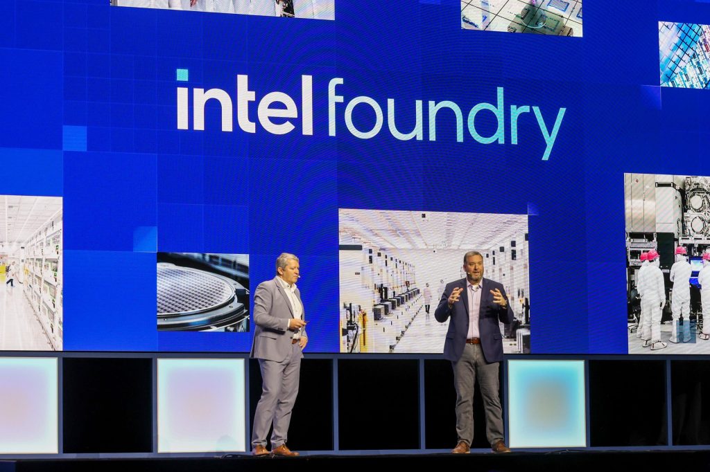
Intel has officially announced that its advanced 18A fabrication process has commenced “risk production.” This significant milestone indicates that large-scale production could soon follow.
Anticipated Technical Advancements with Intel’s 18A Process
The announcement came during the recent Intel Vision 2025 conference, where it was shared that the mass production of the 18A node is slated for late this year. The 18A process holds potential for Intel Foundry Services, which has faced challenges in recent years. This new node is expected to revitalize the division’s prospects.
Risk production is a crucial phase preceding mass production, involving limited initial runs to evaluate the manufacturability and performance of a new process. This stage aims to identify any production line flaws and establish yield rates, which are essential for successful mainstream deployment. Intel’s transition to risk production suggests confidence that the 18A process has addressed previous challenges and is ready for market introduction.
Initial integration of the 18A process will likely occur in Intel’s Panther Lake system-on-chips (SoCs), expected to enter retail markets in 2026. This timeline will provide a critical opportunity to assess the effectiveness of the 18A technology.
Among the notable advancements of the 18A node is the adoption of Backside Power Delivery (BSPDN), which moves power delivery functions to the back of the wafer. The 18A high-density versions reportedly achieve a macro bit density of 38.1 Mb/mm², reflecting promising developments in this technology. Overall, there is optimism surrounding the future of Intel’s 18A process within the increasingly competitive semiconductor landscape.

